外部重繪參考圖
科學影像
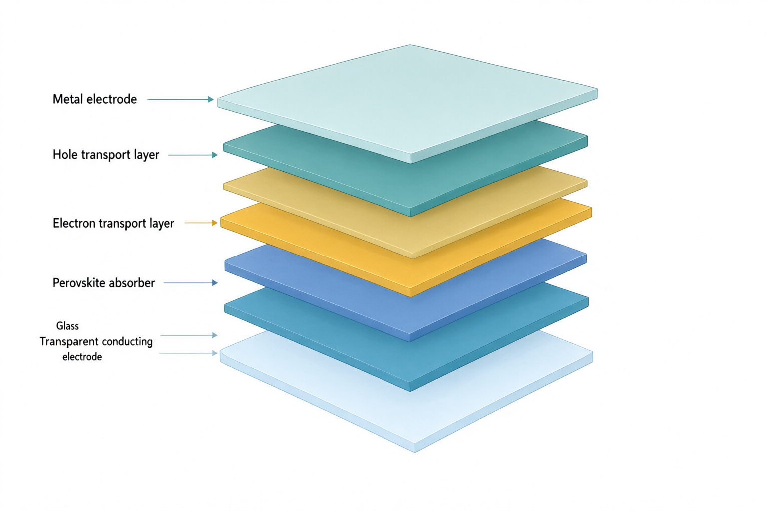
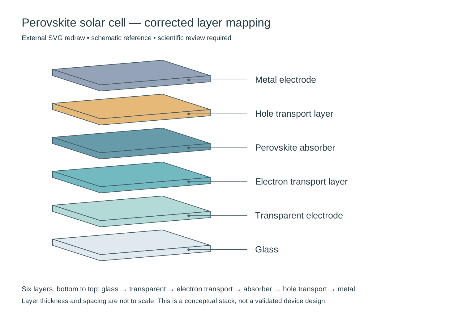
Perovskite solar cell layers
檢查說明
Needs correction: the output adds a seventh slab and does not preserve the requested layer-to-label mapping. In particular, check the electron-transport/perovskite order and the two bottom labels. This is a composition draft, not a validated device architecture; thickness is not to scale.
外部重繪參考圖
Removed the extra slab, restored the requested six-layer sequence and attached each leader to its matching layer. Thickness and spacing remain schematic; this does not validate a particular device architecture.
輸入與確認內容
- 研究概念
- An exploded three-quarter cutaway of a conceptual planar perovskite solar cell. Show exactly six separate solid flat slabs, one slab per material, with equal gaps and no internal textures or additional sublayers.
- 需要包含的物件
- Glass substrate; transparent conducting electrode; electron transport layer; perovskite absorber; hole transport layer; metal electrode.
- 關係與箭頭
- Stack exactly six layers in the listed order, from glass at the bottom to metal at the top. Connect each label to the middle of its corresponding slab using a thin leader line without arrowheads. Layer thickness is schematic, not to scale.
- 精確標籤文字 · 選填
- Glass; Transparent electrode; Electron transport layer; Perovskite absorber; Hole transport layer; Metal electrode
- 視覺要求 · 選填
- Minimal textbook diagram with ample whitespace and teal, blue and amber colors. Print ONLY the short labels explicitly listed in the content. No subtitles, paragraphs, footnotes or extra words. These are drawing directions, not text to display.